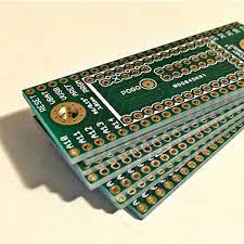
PCB Board Maker
A pcb board maker takes the design of an electronic circuit and converts it to something that can be manufactured. This is a highly complicated process that requires several stages and a large amount of expertise and equipment. The final product is a printed circuit board (PCB), sometimes known as a printed wiring board or etched wire board. The PCB includes copper traces that connect the components to each other and to the power and ground planes on the backside of the board.
PCB fabrication starts with the creation of films that map out the circuit’s blueprint on a piece of laminate material, also called substrate material. This film is affixed to the substrate with copper foil pre-bonded to it, giving it a sturdy structure that is dust-resistant. Then it goes through etching to whittle away the copper where the schematic shows it should go, leaving behind a structure that is an actual printed circuit board.
The bare copper surface is then treated with photoresist, which is imaged (exposed to light through a mask) and developed, removing the unexposed area. The exposed areas are then “sensitized,” making them capable of bonding metal ions in an electrochemical bath. The copper is then plated onto the sensitized areas, forming the circuit board’s conductors. Once the plating is complete the resist mask is stripped.
For multi-layer boards, the next step is to add additional internal layers of copper and insulation. This makes it easier to route electrical connections and reduces signal interference, electromagnetic emissions (EMI), and power supply decoupling. The most common insulation used today is FR-4 glass epoxy, but polyimide and other materials are available.
What is a PCB Board Maker?
Before the invention of the modern printed circuit board, most electronics devices were built from a large number of wires connected to each other using a tag type of assembly. These devices were often expensive, unreliable, and difficult to repair. Modern PCBs are more reliable and can be mass-produced.
In order to avoid problems during manufacturing, a pcb board maker performs an inspection of the bare circuit board before lamination. This is done by an automatic optical inspection machine which compares the digital image of the circuit board with the physical object, detecting any errors. These errors can be corrected before lamination by adding missing copper or removing excess, reducing the time and cost of the PCB.
After the pcb board is completed, it can be soldered to electronic component parts using a pick-and-place machine or bulk wave soldering for through-hole components. It can also be assembled by hand, which is still used for high-volume production and for certain components such as BGA packages. Technicians can also rework and replace failed components, which is called rework.
Once a circuit board is fully populated with components, it is tested to ensure that the electrical components work as intended. This is known as in-circuit testing, analog signature analysis, and functional test. The finished product is then packaged and sold.