Integral to Pcba Printed Circuit Board
The process of assembling the components and traces that enable a printed circuit board to work is integral to Pcba printed circuit board. Testing processes are also vital to the successful completion of a project. Without these procedures, the final product may fail or not function as intended, leading to costly delays. Knowing what testing methods are integral to a PCBA manufacturing project can help engineers and designers make informed decisions that ensure the highest quality and reliability of the finished product.
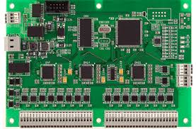
The first step in the PCBA assembly process is known as printed circuit board pcba stuffing. In this phase, components are placed and soldered into position one by one using a machine that recognizes each part as it is inserted. This step is essential to ensure proper component placement and accurate electrical connections.
Once all the parts are in place, copper traces are routed to connect all of the components together and provide an electrical pathway for power or signals to flow through the device. This step can be manual with exploratory data analysis (EDA), or automatic with design software. Accurate trace routing is essential for optimal device performance, and it can be further refined through the addition of labels and identification markings.
What Testing Processes Are Integral to Pcba Printed Circuit Board?
Next comes the visual inspection stage, which can be done manually with the naked eye or magnification tools, or through automated optical inspection (AOI). AOI machines use cameras to scan the surface of the device and detect flaws like misaligned components, solder bridges, and missing or damaged parts. This technique is particularly useful in high-volume production, as it can identify issues more quickly than humans can. However, AOI cannot identify faults that are not visible to the human eye or concealed beneath other components, and it can miss defects such as broken traces and oxidized copper.
Automated X-ray inspection (AXI) is another powerful tool used to check the integrity of a PCBA’s traces, pads, and connections. AXI systems can detect issues that are invisible to the naked eye, including buried vias and blind vias. This method is also very effective in detecting solder joints that are not properly aligned, broken, or undersized. However, aXI can be time-consuming, and it can require custom test fixtures to be created for each new design.
In-circuit testing (ICT) is a highly accurate and automated method that can verify each component by connecting them to a fixture known as a “bed of nails.” ICT can detect faults such as short circuits, open circuits, and incorrect component values, and it can measure resistance, capacitance, and inductance with high accuracy. This is a more expensive test method, and it requires that each new PCBA be made into a specialized ICT fixture.
Burn-in testing is a more intense type of test designed to establish a device’s load capacity by pushing power through the components and connections at their maximum-specified capacity. This type of test is especially useful for devices that must perform flawlessly in harsh environments, such as military and medical equipment. The downside of this test is that it can significantly reduce the lifespan of components and connections by stressing them beyond their rated capacity.