Role of Vias in RF PCB Design
RF (radio frequency) PCBs require high-speed signal transfer that can happen on multiple layers of the circuit board. This type of PCB is more complex than a standard one and is sensitive to issues like impedance matching, noise reduction, and interference. Due to this, it is vital that engineers use proper techniques when creating their RF PCB designs. This includes ensuring that the PCB stack-up is properly configured, using the correct dielectric material, reducing impedance fluctuations through bends and corners in transmission lines, and more.
The most important aspect of a rf pcb is the ground plane, which reduces interference or noise and provides a low-impedance return path for signal currents. Using the right grounding technique can also help prevent coupling between traces and other components. This is crucial in reducing electromagnetic interference (EMI) and electromagnetic compatibility (EMC) concerns.
Another critical feature of an RF PCB is the layer arrangement and the order of different conductive and dielectric layers. Typically, the RF layer comes on top of the other layers and is followed by power and ground planes. This layer configuration is crucial for achieving optimal RF performance and is determined by several factors, including the component placement, trace widths, and dielectric materials.
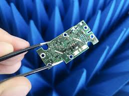
What is the Role of Vias in RF PCB Design?
When routing the RF PCB, it is crucial to keep the transmission lines separated from other traces, especially those carrying high-speed signals. This can be done by following a route that is separated by a layer from the RF traces or by inserting decoupling capacitors.
Additionally, the RF PCB must contain a dedicated ground plane on its component layer. This ensures that DC and RF currents can be returned to the grounding path without adding interference to the other signals on the RF layers.
In addition to this, it is vital that the RF layer has a large number of ground vias added liberally throughout the RF portion of the circuit. These vias will help to prevent the accrual of parasitic ground inductance on traces that have long return paths. It is also recommended that the RF layers be stitched together with ground vias, as this will provide shorter paths for the current to return.
It is important to keep the via diameter small for RF signals, as a larger aspect ratio will lead to higher parasitic inductance. The preferred via size for RF is 0.5 mm (8 mils). The buried vias used in RF PCBs should have a small diameter as well to minimize the amount of digital noise that can leak to RF traces and components. This can be solved by placing the buried vias close to the RF components, minimizing the number of layers they pass through. This will also decrease the chances of the buried vias coupling with other signals passing through them. This will lead to a more efficient and stable RF circuit.