Buried Via Hole Be Filled With Conductive Paste
A PCB via hole is a copper-plated hole that creates an electric connection between the different layers of a printed circuit board. The via can be filled with either conductive or non-conductive material, depending on the application and requirements of the circuit board. A common method for filling the via is by using a conductive epoxy, but there are other options as well. Regardless of the type of via, all PCBs require some sort of via-filling process to ensure the integrity of the connection between the layers.
The traditional technology of creating interconnections between layers on a multilayer printed circuit board requires the use of plate through holes, which are drilled completely through the entire PCB and then electroplated with copper and other metals. This method consumes a lot of the PCB surface area and is relatively laborious and expensive. However, there are ways to reduce the need for these large holes by using smaller blind and buried via hole.
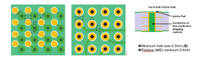
Both blind and buried via holes can be filled with a conductive epoxy. The choice of the epoxy will depend on the needs of the circuit board and will affect how well it can withstand climatic conditions. For example, a circuit board that will be used in a high-temperature environment may require a more durable conductive epoxy than one that will only need to withstand lower temperatures.
Can Buried Via Hole Be Filled With Conductive Paste?
Using a conductive epoxy to fill a buried or blind via can significantly improve the efficiency of the hole and help ensure that it is fully functional. Conductive epoxy can also increase the thermal conductivity of the hole, which can help to deviate the heat from larger components and reduce the risk of shorting or other problems.
Buried and blind via holes can be a useful option for increasing the density of a multilayer PCB, but there are some things to keep in mind when designing a PCB that will have these types of holes. For instance, it is important to make sure that the buried and blind vias are positioned correctly in the board’s design, as this can have a significant impact on the overall electrical performance of the circuit board.
The buried and blind vias in a multilayer PCB must be carefully fabricated, as the process of drilling them is much more complex than the standard plated through hole process. This is because the buried and blind vias do not connect to the surface of the PCB, so they must be drilled in between the inner layer pads. This requires the use of a special drill that can be positioned exactly where the inner layers need to be connected. In addition, the holes must be plated before the inner layers are bonded together. This is a very laborious and costly process, but it is essential for the successful production of a multilayer PCB that uses blind and buried vias.