PCB manufacturing address high-density designs
As technology advances, the demand for high-density printed circuit boards (PCBs) has surged, driven by the need for more compact and powerful electronic devices. High-density designs feature tightly packed components and intricate circuit layouts, which pose unique challenges for PCB manufacturers. However, various techniques and innovations have been developed to address these challenges effectively, enabling the production of high-performance PCBs that meet the rigorous demands of modern applications.
One of the primary approaches to achieving high-density designs in pcb manufacturing is the reduction of trace widths and spacing between conductive paths. Traditional PCBs may use wider traces, but high-density designs require narrower traces to accommodate more components in a limited space. Manufacturers employ advanced photolithography techniques to create precise patterns on the PCB substrate. This process allows for the etching of ultra-fine traces that are often less than 100 microns wide, significantly increasing the board’s capacity for components while maintaining electrical integrity.
Another essential aspect of addressing high-density designs is the use of multi-layer PCBs. In contrast to single-layer boards, multi-layer PCBs stack several layers of circuitry, allowing for more complex designs without increasing the board’s footprint. Each layer is carefully designed and fabricated, with vias (small holes) used to connect traces across different layers. This layering approach not only maximizes space but also improves signal integrity by minimizing the length of traces and reducing electromagnetic interference. Advanced technologies, such as blind and buried vias, further enhance design flexibility by allowing connections to be made between specific layers without penetrating all layers of the PCB.
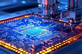
How does PCB manufacturing address high-density designs?
To accommodate the high-density requirements of modern devices, PCB manufacturers have also adopted surface mount technology (SMT). SMT components are significantly smaller than traditional through-hole components, allowing for greater packing density. With SMT, components are mounted directly onto the surface of the PCB rather than through holes, enabling designers to utilize the available space more efficiently. Additionally, automated placement machines can quickly and accurately position these small components, enhancing production efficiency and consistency.
Thermal management is another crucial consideration in high-density PCB designs. As components are packed more closely together, they generate heat, which can lead to performance issues and reliability concerns. Manufacturers address this challenge by incorporating thermal vias, heat sinks, and advanced materials with better thermal conductivity. These solutions help dissipate heat effectively, ensuring that the PCB operates within safe temperature limits, thus enhancing overall performance and longevity.
Moreover, the choice of materials plays a significant role in supporting high-density designs. Manufacturers often use high-frequency substrates with low dielectric constants and low loss tangents, which are essential for maintaining signal integrity in densely packed circuits. These materials reduce signal loss and crosstalk, which are critical for the performance of high-speed electronic devices. Innovations in materials science have led to the development of flexible and rigid-flex PCBs, further expanding design possibilities for high-density applications.
Lastly, the increasing complexity of designs necessitates robust design software and tools for PCB layout. Advanced computer-aided design (CAD) software enables engineers to simulate and optimize high-density layouts, ensuring that the design meets electrical and mechanical requirements before manufacturing begins. These tools help identify potential issues such as signal integrity problems and thermal hotspots, allowing for proactive solutions that enhance the final product’s performance.
In conclusion, PCB manufacturing addresses high-density designs through a combination of advanced technologies, innovative materials, and design practices. By employing techniques such as fine trace etching, multi-layer construction, surface mount technology, and effective thermal management, manufacturers can produce PCBs that meet the growing demands of modern electronics. As devices continue to shrink while becoming more powerful, the ability to design and manufacture high-density PCBs will remain a critical aspect of the electronics industry’s evolution.